117
FRAUNHOFER INSTITUTE FOR MICROSTRUCTURE OF MATERIALS AND SYSTEMS IMWS/
CENTER FOR APPLIED MICROSTRUCTURE DIAGNOSTICS CAM
About Fraunhofer IMWS/CAM
Fraunhofer IMWS/CAM is a leading ser-
vice provider for failure diagnostics and
materials assessment. Contract R & D
for industry in the area of semiconduc-
tor technologies, microelectronic com-
ponents, microsystems and nanostruc-
tured materials is our day-to-day business.
Fraunhofer CAM covers the entire work
flow from non-destructive defect locali-
zation over high precision target prepara-
tion to cutting edge nanoanalytics, sup-
plemented by micro-mechanical testing
and numerical simulation. In preparation
for future challenges, we do undertake
intense forefront research in cooperation
with international partners from academia
and industry. See
for further information.
Failure Diagnostics in Power
Electronics
Fraunhofer IMWS/CAM provides failure
analysis for power semiconductors,
including power ICs, MOS transistors,
IGBTs, diodes and sensors developed for
operation under standard and harsh envi-
ronment. In addition to Si-based systems,
we investigate and analyze the behavior
and performance characteristics of novel
SiC and GaN based devices including
related dielectrics, metallization layers
and contact systems.
Particular attention is paid to a fundamen-
tal understanding of interface material
properties and mechanisms relevant for
new interconnection and packaging
approaches. Current activities cover the
characterization of heavy wire bonding
materials, Ag-sintering, diffusion solder-
ing, new substrates and housing materials.
Fraunhofer CAM closely collaborates with
leading manufacturers of analysis and
testing equipment with explicit focus on
the development of innovative tools and
test methods for quality assessment and
failure analysis valuable for the electron-
ics industry.
Portfolio
•
Microstructure/failure analysis of power
semiconductors on wafer and chip level
(ICs, MOS transistors, IGBTs, diodes
based on Si, SiC and GaN) and of pack-
aged components and modules
(including high temperature operation
> 250°C)
•
Material characterization of high
temperature-stable metallization and
conducting systems
•
Characterization of interconnection
materials like heavy wire bonding
contacts/materials (e.g. Al, Cu, Al/Cu
clad wires/ribbons)
•
Characterization of encapsulation
and housing materials
•
Modeling and numerical simulation
of mechanical, thermal and thermo-
mechanical device and material
properties
•
Development of tools and methods
for failure diagnostics and quality
assessment specifically adapted to
power electronics
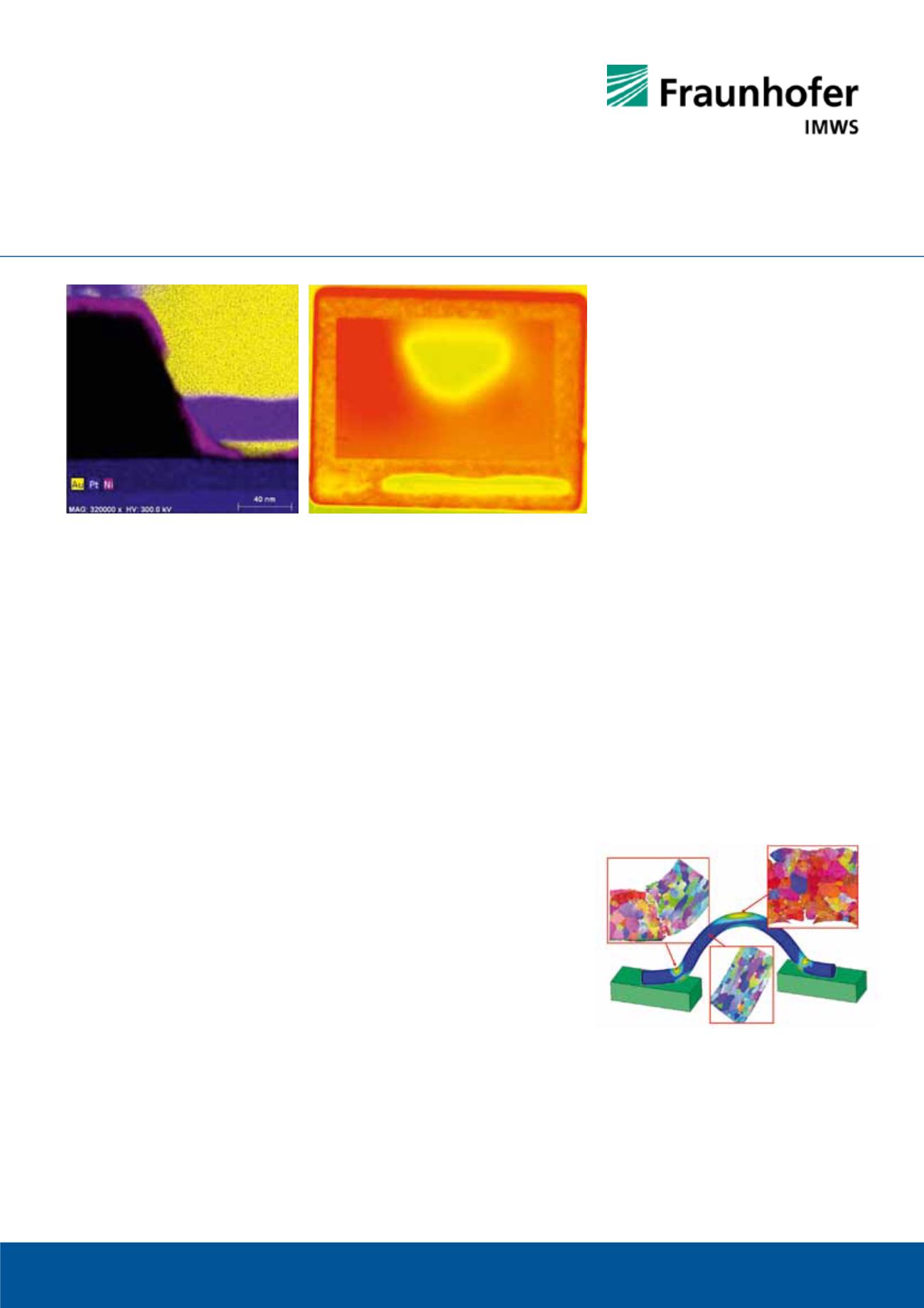
TEM EDS mapping of a GaN HEMT gate structure
Pulsed thermography of a defective Power MOSFET
device with interface delamination
Finite Element model and grain structure characteri-
zation by Electron Backscattered Diffraction (EBSD)
for a low cycle fatigue analysis of heavy wire
bonding interconnects


