112
Fraunhofer Institute for Applied Solid State Physics IAF
About
The Fraunhofer Institute for Applied Solid
State Physics IAF in Freiburg is one of the
world’s leading research institutes in III/V
semiconductor technology and modules.
Within its five business units Power Elec-
tronics takes a leading role. Fraunhofer IAF
develops energy-efficient solutions for en-
ergy conversion, broadband communica-
tion systems, high data rate transmission,
imaging, detectors as well as semicon-
ductor lasers. In cooperation with a broad
range of international project partners,
Fraunhofer IAF performs its expertise
material and process technology, in chip
design, and in the manufacturing of
devices and modules. In 2015, the insti-
tute had 280 employees including more
than 30 PhD students.
Power Electronics at IAF
Power electronics at IAF is based on the
development of Gallium Nitride (GaN) on
up to eight inch silicon and diamond elec-
tronics, both with GaN on diamond sub-
strates, and on the longer term, real dia-
mond electronics. Overall, GaN-based
devices on Silicon already have a direct im-
pact on future efficient power conversion
systems and will thus help save energy
and miniaturize systems. GaN technology
is promising for automotive, photovoltaic,
IT- and consumer applications as well as
motor control and appliances. Based on
the longstanding experience and the suc-
cessful industrialization of GaN RF-pro-
cesses in Europe Fraunhofer IAF in power
electronics concentrates on the critical
aspects of:
•
Defect-reduced material growth up to
8-inches in diameter,
•
Process development with a focus on
integration for fast switching,
•
In-depth characterization, chip-related
packaging, EMC, and reliability.
The needs for ever-higher transistor per-
formances and reliability drive a continu-
ous search for improved epitaxy, process
technology, and advanced characteriza-
tion. GaN on diamond in wafer transfer
approaches and, generically as a semi-
conductor material with ultimate perfor-
mances are being developed for improved
thermal performances. For pure diamond
electronics, baseline growth of diamond
and processes are under development.
Epitaxy
GaN-based devices with generically a
wider bandgap than silicon have a much
higher critical electrical field and, together
with high carrier concentration and high
mobility, they offer superior trade-off of
specific on-state resistance R
DS(ON)
versus
breakdown voltage rating and show low
switching losses. For GaN to be cost effec-
tive silicon reenters GaN devices as a sub-
strate material with large diameters, which
is a challenge regarding defect reduction,
overall material quality, and overall pro-
cess yield. Fraunhofer IAF optimizes mate-
rial growth with a strong focus on mate-
rial characterization on improved growth
schemes and machines.
Process Development and Reliability
IAF’s baseline AlGaN/GaN high-voltage
process technology is based on devices
with standard 0.5 μm gate lengths. We
pursue performance and reliability im-
provements of AlGaN/GaN-based devices
for various voltage classes up to at least
1200 V and currents currently as high as
200 A per chip.
Characterization
IAF concentrates on the characterization
of the static and losses on devices level,
on critical defects, on EMC for the pro-
posed increase of the switching speed of
the GaN-based converters to the 10 MHz
range, e.g. using multilevel converters.
Starting from the material growth reliabil-
ity is the central aspects for high-power-
density devices, currently for large-area
devices. We expect GaN to evolve in pow-
er electronics driving performances to un-
precedented levels in converters and to
open new applications and cost perfor-
mance trade-offs.
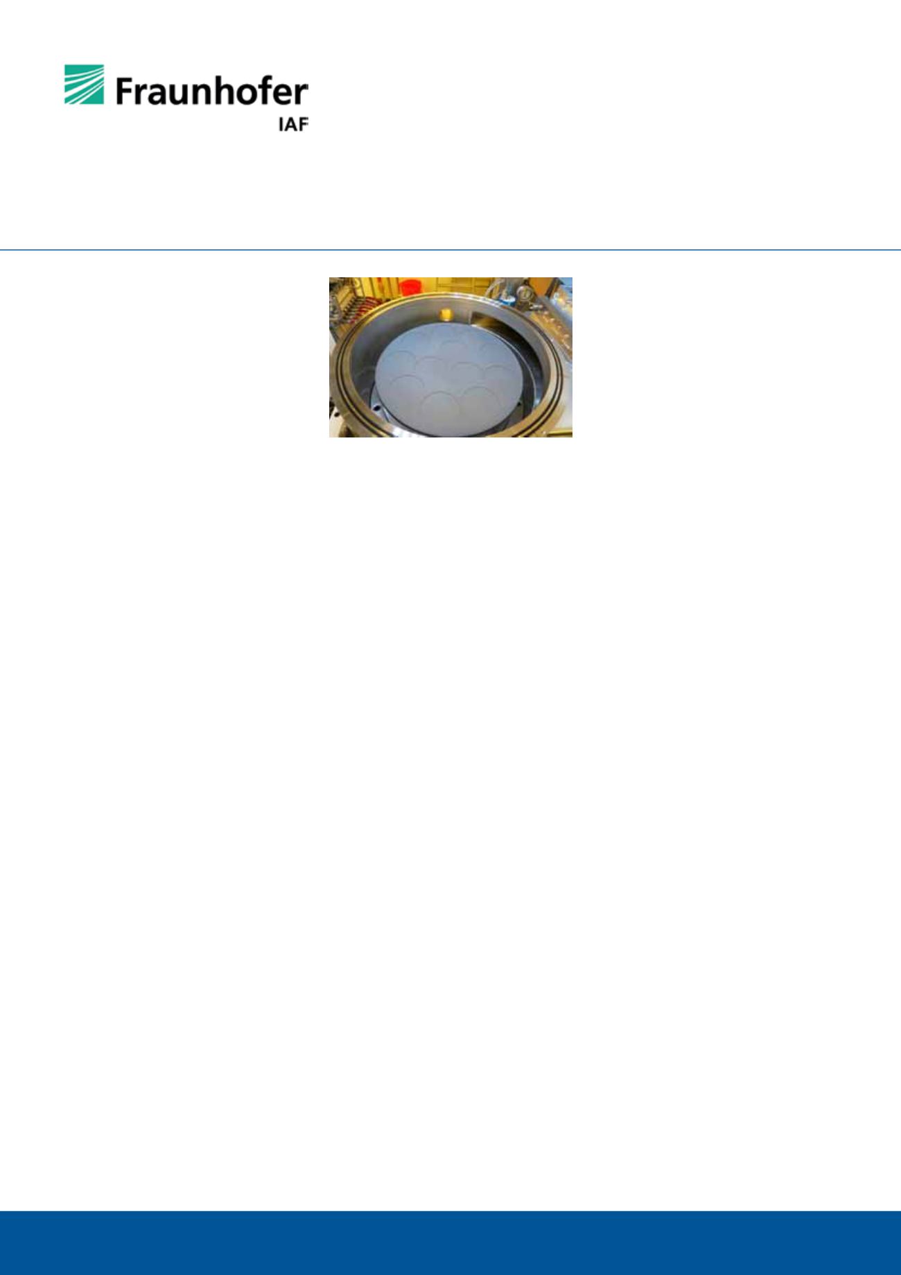
Multiwafer MOCVD growth machine for up to
8-inch growth of GaN on Silicon.


