129
General Information
The University of Applied Sciences in
Kempten is located in the south of Ger-
many, close to the Bavarian Alps. The
institution was founded in 1977 to es-
tablish a regional center for academic
education in the Allgäu area. Today, the
University of Applied Sciences Kempten
has roughly 6000 students, of whom
1000 are enrolled at the department of
Electrical Engineering in different Bache-
lor and Master programs.
Laboratory for Electronics Integration
The Laboratory of Electronics Integration
(EI-Lab) was founded in 2015 to pro-
mote applied research and education in
the field of electronics packaging, mi-
cro-integration, and thermal manage-
ment. Currently, the lab comprises an in-
terdisciplinary team of seven scientists,
engineers, and technicians. The team is
supported by numerous students, who
perform their student or thesis project
within the lab. Both, public and indus-
try funded research projects are carried
out by the staff and concern the follow-
ing topics:
1.
PCB embedding of power semicon-
ductors:
Ongoing research projects fo-
cus on embedding of 1200V IGBT and
diode chips in printed circuit boards.
Reference applications are motor drives
with nominal output powers in the
range of 5 to 50 kW.
2.
Design and fabrication of PCB
based microsystems:
Embedding of
piezoelectric materials in printed cir-
cuit boards opens up the potential for
many new, highly integrated, mini-/
micro-electromechanical systems. A
piezoelectric vibration energy harvest-
er has been designed, fabricated, and
tested as first proof-of-concept.
3.
Thermal management of (power)
electronic systems:
The lab offers its
expertise in heat transfer and CFD sim-
ulations for development and consult-
ing activities for industry partners.
For these activities, the lab provides an
extensive infrastructure. Core of the lab
equipment is a prototyping line for print-
ed circuit boards that comprises a circuit
board plotter, spray etcher, via plater,
and multilayer press. For semiconduc-
tor packaging the lab is equipped with
a clean bench, sinter press, wire bonder,
vacuum evaporation machine, and equip-
ment for polymer casting. To character-
ize samples fabricated in the lab several
optical microscopes, a scanning electron
microscope and a test setup for power
semiconductor characterization (static,
dynamic, thermal) are available. State-of-
the-art software tools for CAD, FEM/CFD,
circuit design and analysis are used for
designing lab-scale demonstrators.
Demonstrator of PCB-based piezoelectric vibration
energy harvester
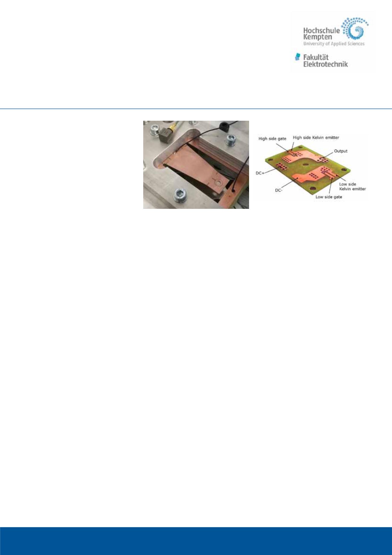
1200V/25A PCB embedded IGBT half bridge
fabricated at EI-Lab.
Hochschule Kempten


