96
The Institute
The Institute for Microelectronics and
Microsystems (IMM) belongs to the
Physics and Matter Technologies Depart-
ment (DSFTM) of the National Research
Council of Italy (CNR), the largest Italian
public research organization. IMM has
the headquarters in Catania and research
units located in Agrate, Bologna, Rome,
Naples, Lecce and Catania. The Institute
has a permanent staff of about 200
people, with expertise in physics, chem-
istry and electronics engineering. The
temporary staff counts also several Post-
Docs and Ph.D. students.
The research activity is focused on innova-
tive solutions for micro and nanoelectron-
ics, advanced materials and processing for
smart components, optoelectronics and
photonics, sensors and multifunctional
micro/nanosystems. In particular, IMM has
a recognized experience on wide band
gap semiconductors (SiC and GaN) device
processing and physics, carrying out fun-
damental research with important impli-
cations in power electronics.
Key research fields and competence
areas
The main research interests and compe-
tences are focused on the physics of SiC
and GaN power devices (Schottky diodes,
JBS, MOSFETs. HEMTs, MISHFETs,
MOSHEMTs,…), including materials,
processing and devices behavior. The
key research topics include:
•
Physics of metal/semiconductor inter-
faces (Ohmic and Schottky contacts)
•
Transport phenomena at dielectrics/
semiconductors interfaces
•
Carrier profiling after doping and
activation
•
Post-oxidation annealing of gate oxides
and mobility in WBG transistors.
•
Atomic Layer Deposition (ALD) of novel
dielectrics materials
•
Integration of 2D materials (like gra-
phene, MoS2, …) on WBG devices
technology
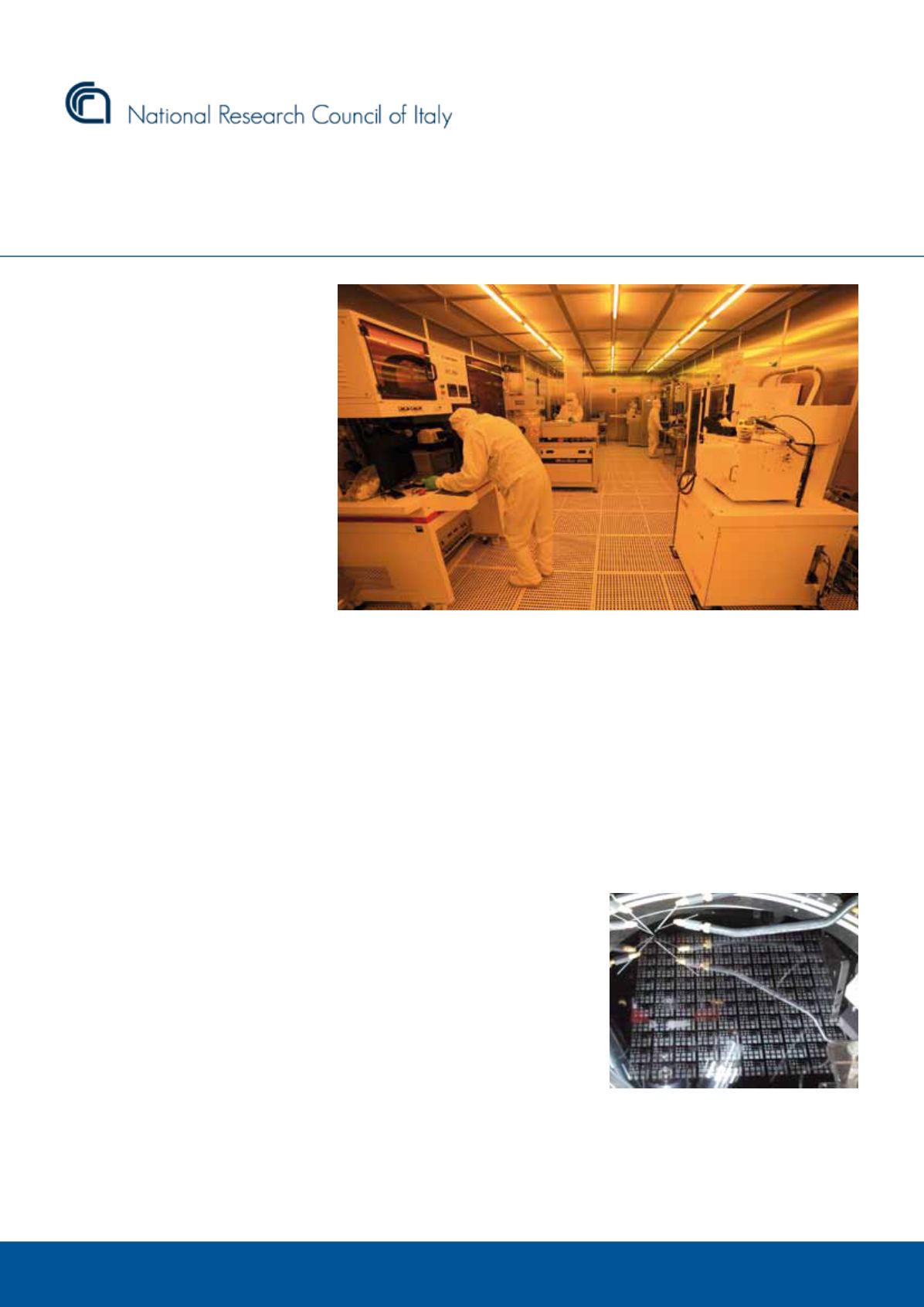
Facilities and highlights
The research activity takes advantage of
the facilities of the Institute, in particular,
of a clean room equipped for lithography
(direct laser writing, e-beam and nano-
imprinting lithography), etching (plasma
etchers with F and Cl chemistry, dedicated
National Research Council of Italy (CNR)
wet benches), thermal processes (conven-
tional and rapid annealing furnaces), metal
layer deposition (multi-target sputters and
evaporation systems), atomic layer depo-
sition. Moreover, the Institute holds com-
petencies and equipments to carry out a
wide range of advanced morphological,
structural and electrical characterizations
(TEM, XRD, AFM, SPM, Hall, I-V, C-V,...),
required in power electronics devices
technologies.


