87
Ferdinand-Braun-Institut Berlin
FBH’s Portfolio
The FBH is an internationally recognized
competence center for optoelectron-
ic and electronic research based on III-V
compound semiconductors. It operates
industry-compatible and flexible clean
room laboratories with vapor phase epi-
taxy units for the growth of GaAs- and
GaN-based epitaxial structures and a III-V
semiconductor process line for wafer di-
ameters up to 4 inches. The work relies
on comprehensive materials and process
analysis equipment, a state-of-the-art de-
vice measurement environment, and ex-
cellent tools for simulation and CAD. In
close cooperation with industry, its re-
search results lead to cutting-edge prod-
ucts.
GaN Power Electronics at FBH
Gallium nitride (GaN) is characterized
by its excellent dielectric breakdown
strength. Thus, GaN-based High Electron
Mobility Transistors (HEMTs) offer excel-
lent power densities and combine high
electron mobility with high saturation ve-
locity. They are therefore well-suited for
high frequencies, high voltages and very
fast and low loss (efficient) switching ap-
plications.
Innovative devices for power electron-
ic applications aim at achieving fast and
efficient high-voltage switching capa-
bilities combined with normally-off be-
havior. Our developments towards GaN
power HEMTs focus on increasing the
breakdown voltage up to 1000 V. Further
objectives are to develop and realize de-
vice concepts for low on-state resistances
down to 10 m cm² as well as for normal-
ly-off devices. Accordingly, we optimize
epitaxial designs and growth procedures
as well as technological parameters and
specific features such as field plates, pas-
sivation layers, and layout designs com-
patible to high-voltage applications.
By concentrating electrons in the transis-
tor channel, high breakdown voltages are
achieved. Thus, corresponding epitaxial
layer designs are used providing a repel-
ling electrostatic force to the electrons
(back barrier designs). For normally-off
GaN power transistors, we are focusing
on p-GaN gate technology. This technol-
ogy renders the intrinsic potential distri-
bution close to the gate such that the de-
vices can only be switched on at positive
voltage. A threshold voltage of +1.5 V and
a gate dynamic range of +5 V are charac-
teristic values. Our high-current transis-
tors up to 150 A rely on a two-dimen-
sional scaling of the transistor width
considering thermal issues and combin-
ing it with flip-chip mounting capability.
The combination of these properties
qualifies FBH transistors for power ap-
plications in automotive electronics, ter-
restrial and space-borne solar converter
technology and others.
We are actively involved in various pro-
jects funded by industrial as well as pub-
lic national and European sources.
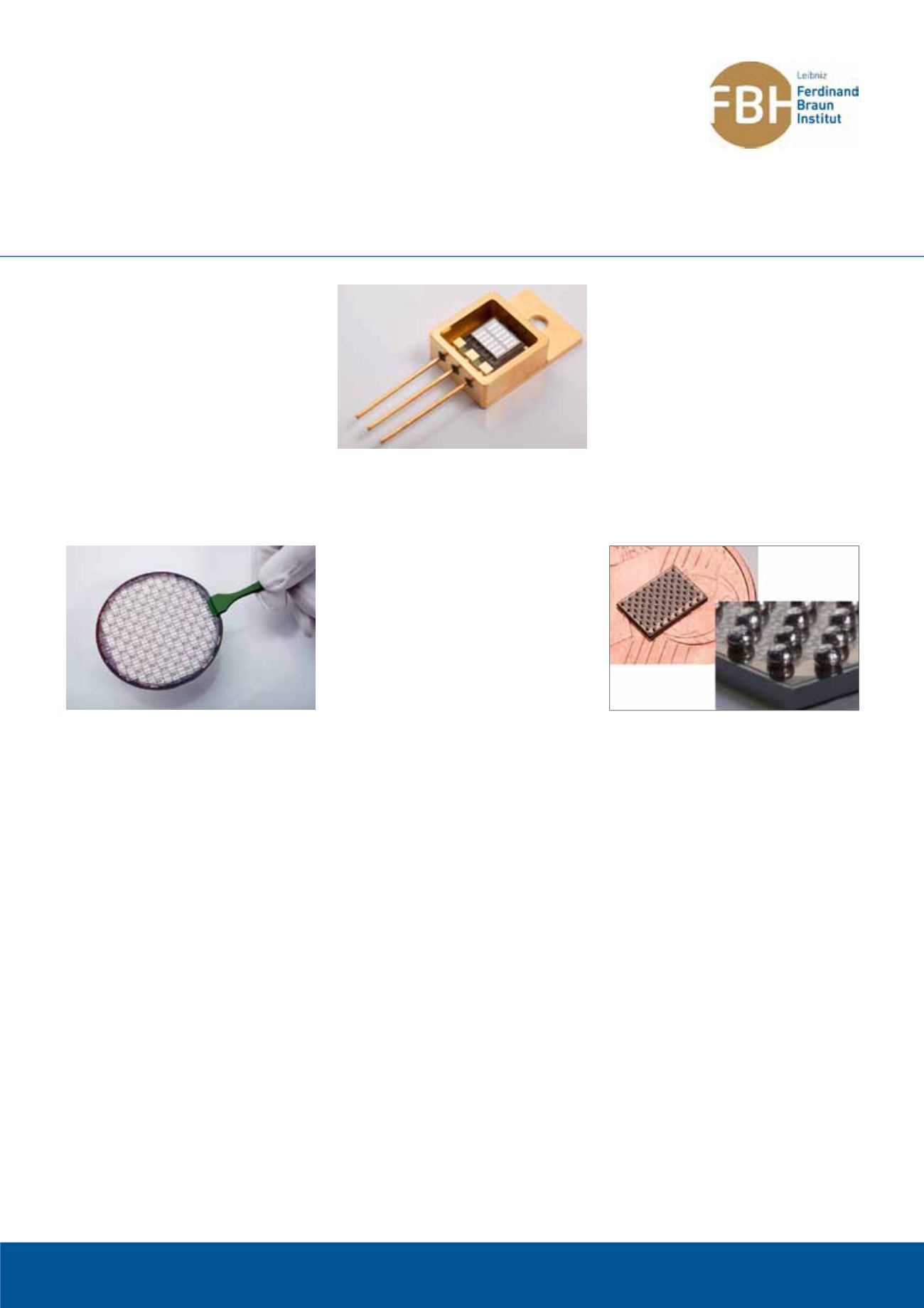
Processed GaN-on-SiC wafer containing power
transistor chips
Flip-chip mounted 50 A/ 250 V normally-off GaN
power transistor
250 V / 75 A GaN power transistor optimized for
flip-chip mounting GaN power transistor


